| You are not Logged In! |
Difference between revisions of "Public:Layout Standards"
m (images again. they format weird) |
Adam Kaszok (talk | contribs) m (dude this formatting pmo) |
||
| (28 intermediate revisions by 6 users not shown) | |||
| Line 1: | Line 1: | ||
| − | |||
| − | |||
''See [[Schematic Conventions]] for related information about developing your schematic properly before you venture to the layout.'' | ''See [[Schematic Conventions]] for related information about developing your schematic properly before you venture to the layout.'' | ||
| Line 7: | Line 5: | ||
{{RemarksBox Warn|Title=Under Construction|Text=All content below this point is under construction. Follow all conventions given here and be aware they may not cover all situations.}} | {{RemarksBox Warn|Title=Under Construction|Text=All content below this point is under construction. Follow all conventions given here and be aware they may not cover all situations.}} | ||
| − | {{RemarksBox Info|Title=Note for KiCad | + | {{RemarksBox Info|Title=Note for KiCad 7|Text=The latest versions of KiCad include a few differences in settings from the older versions. Since we are all using the latest version, please be aware there may be settings you can't find and update these instructions as you find any changes in the software.}} |
| − | {{RemarksBox Info|Title=Units|Text=Millimeters are fantastic and we encourage using metric dimensions whenever possible, however [https://bayareacircuits.com/capabilities/ | + | {{RemarksBox Info|Title=Units|Text=Millimeters are fantastic and we encourage using metric dimensions whenever possible, however [https://bayareacircuits.com/capabilities/ BAC's standard capabilities] are written in mils (1/1000 inch) or inches so we present all minimum and recommended dimensions in both mm and mil.}} |
| − | + | __TOC__ | |
| − | |||
| − | |||
| − | |||
| − | |||
=General Settings= | =General Settings= | ||
| Line 23: | Line 17: | ||
These dimensions can be set in the "'''Setup -> Design Rules...'''" dialog box. Below are the recommended values for the default net class, and you will likely want to increase them for traces that will carry considerable amounts of current. Don't worry about the settings for microvias (µvias), which we don't use at ISC since they cost extra money to fabricate. | These dimensions can be set in the "'''Setup -> Design Rules...'''" dialog box. Below are the recommended values for the default net class, and you will likely want to increase them for traces that will carry considerable amounts of current. Don't worry about the settings for microvias (µvias), which we don't use at ISC since they cost extra money to fabricate. | ||
| − | {| | + | {| class="wikitable" |
|'''Dimension''' | |'''Dimension''' | ||
|'''mil''' | |'''mil''' | ||
|'''mm''' | |'''mm''' | ||
|- | |- | ||
| − | | | + | |Minimum clearance |
|6 mil | |6 mil | ||
|0.1524mm | |0.1524mm | ||
|- | |- | ||
| − | |Track Width | + | |Minimum Track Width |
|6 mil | |6 mil | ||
|0.1524mm | |0.1524mm | ||
|- | |- | ||
| − | | | + | |Minimum Connection Width |
| − | | | + | |0 mil |
| − | | | + | |0mm |
|- | |- | ||
| − | |Via Dia | + | |Minimum Via Dia |
|27.55901575 mil | |27.55901575 mil | ||
|0.7mm | |0.7mm | ||
|- | |- | ||
| − | |Via Drill | + | |Copper to edge clearance |
| + | |10 mil | ||
| + | |0.254mm | ||
| + | |- | ||
| + | |Minimum through hole (Via Drill) | ||
|11.81098425 mil | |11.81098425 mil | ||
|0.3mm | |0.3mm | ||
| + | |- | ||
| + | |Minimum thermal relief spoke | ||
| + | |1 spoke | ||
| + | |1 spoke | ||
| + | |- | ||
| + | |Track Width Rec. | ||
| + | |8 mil | ||
| + | |0.2032mm | ||
|} | |} | ||
These values are suggested minimum values, and can be increased. Feel free to round numbers up. When increasing the via drill size, it is important to increase the via diameter as well, because the difference between the two must be greater than 10 mil ''(0.254mm)'' to meet BAC's 5 mil ''(0.127mm)'' minimum annular ring requirement. The picture below illustrates what the different dimensions mean. | These values are suggested minimum values, and can be increased. Feel free to round numbers up. When increasing the via drill size, it is important to increase the via diameter as well, because the difference between the two must be greater than 10 mil ''(0.254mm)'' to meet BAC's 5 mil ''(0.127mm)'' minimum annular ring requirement. The picture below illustrates what the different dimensions mean. | ||
| − | |||
| − | Here | + | [[File:Annular_Ring.jpg|frameless|145x145px]] |
| − | [[File: | + | |
| + | Here are two screenshots of part of the dialog box with the dimensions set. For new designs/revisions, go with the first image. To edit them for your project, simply click on a cell in the table and start typing the new dimension. You are free to double click and copy-paste dimensions from one cell to another. [[File:Constraint Settings KiCAD v9.png|768x768px|alt=|thumb|Settings for KiCad 9 '''(USE THESE FOR NEW DESIGNS!)'''|none]] | ||
| + | [[File:Board_Constraints_KiCad_v7.png|alt=|770x770px|thumb|Legacy settings (older boards may have these settings)|none]] | ||
==Copper Pours== | ==Copper Pours== | ||
| − | + | {{RemarksBox Info|Title=Note for KiCad 7|Text=These settings do not need to be applied to pass BAC DFM, KiCad v7 default should suffice}} | |
Also known as copper planes, zones (used in KiCad), or a ground plane, copper pours can greatly ease PCB layout and increase PCB performance. To access these settings, you can mouse over any existing copper zone and edit the zone properties. If you are placing a new zone, the options will pop up for the new zone before you can start placing it. These values are set for each copper pour separately, although you can use the "export setting to other zones" button to change the settings of all other pours to match. | Also known as copper planes, zones (used in KiCad), or a ground plane, copper pours can greatly ease PCB layout and increase PCB performance. To access these settings, you can mouse over any existing copper zone and edit the zone properties. If you are placing a new zone, the options will pop up for the new zone before you can start placing it. These values are set for each copper pour separately, although you can use the "export setting to other zones" button to change the settings of all other pours to match. | ||
* Clearance: 0.2mm | * Clearance: 0.2mm | ||
| Line 110: | Line 117: | ||
** You can just print out a schematic or [[KiCad BOM|BOM]] to reference while soldering. | ** You can just print out a schematic or [[KiCad BOM|BOM]] to reference while soldering. | ||
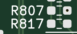
* Put the reference designator (RefDes) on top of the component lengthwise like this: | * Put the reference designator (RefDes) on top of the component lengthwise like this: | ||
| − | [[File: | + | [[File:Ref_des_placement.png|frameless]] [[File:RefDes3.png|frameless|186x186px]] |
| + | * If that position is not possible, orient RefDes like this | ||
| + | * [[File:RefDes2.png|left|alt=|frame]][[File:RefDes4.png|frameless|175x175px]] | ||
| + | * If neither is possible, use best judgement, but remain consistent | ||
* Headers | * Headers | ||
** All header pins must be labeled with the name of the signal that they are transmitting | ** All header pins must be labeled with the name of the signal that they are transmitting | ||
| Line 119: | Line 129: | ||
** Release date (MMM/YYYY) | ** Release date (MMM/YYYY) | ||
** Blank box for serial number | ** Blank box for serial number | ||
| − | ** ISC logo | + | ** ISC logo, should be full car silhouette unless absolutely impossible |
| − | ** Sponsor Logos | + | ** Sponsor Logos, until further notice, all boards should have the Bay Area Circuits Logo on the front |
** If necessary, warnings and special precautions | ** If necessary, warnings and special precautions | ||
* Bottom Side: | * Bottom Side: | ||
| Line 132: | Line 142: | ||
Test points make it easier to check signals and voltages on your board. They are a pad or hole in the board that is electrically connected to a signal and allows you to easily probe that signal and check it on a meter or oscilloscope. | Test points make it easier to check signals and voltages on your board. They are a pad or hole in the board that is electrically connected to a signal and allows you to easily probe that signal and check it on a meter or oscilloscope. | ||
| + | |||
| + | ==Git Checks== | ||
| + | |||
| + | All Git pull requests are automatically checked for correctness. Tnis ensures title blocks are correctly made, however these checks sometimes fail without apparent cause. If you cannot resolve the check, try this: [[Git Check Failure]] | ||
==Physical Board Dimensions and Shape== | ==Physical Board Dimensions and Shape== | ||
| Line 152: | Line 166: | ||
** Try to stick to rectangular or square, but it's ok to use a different shape if your project needs it. | ** Try to stick to rectangular or square, but it's ok to use a different shape if your project needs it. | ||
** Corners should be rounded off. Use the arc tool for this until they add rounded rectangles to KiCad. | ** Corners should be rounded off. Use the arc tool for this until they add rounded rectangles to KiCad. | ||
| + | |||
| + | == Gerbers and DFM == | ||
| + | When you are finished or nearly finished with your layout review, you will need to [[KiCad#Export for Manufacturing|generate gerbers]] and run [[Bay Area Circuits#DFM Report|BAC's InstantDFM]]. | ||
=Further Reading= | =Further Reading= | ||
| + | [[Adding_Symbols_%26_Footprints_to_KiCad]] | ||
Bay Area Circuits's [https://bayareacircuits.com/capabilities/ standard capabilities]. | Bay Area Circuits's [https://bayareacircuits.com/capabilities/ standard capabilities]. | ||
Latest revision as of 13:16, 12 March 2026
See Schematic Conventions for related information about developing your schematic properly before you venture to the layout.
Our team is in the process of creating and implementing standards for all of our electrical design and CAD. This is being done in an attempt to reduce errors in manufactured boards, make it easier for other members to edit boards that were already created, and make the finished CAD look presentable. We will also create a KiCad project template to set the DRC (Design Rule Checker) to our standards and make all our boards follow Bay Area Circuits' manufacturing constraints.
| Under Construction | |
| All content below this point is under construction. Follow all conventions given here and be aware they may not cover all situations. | |
| Note for KiCad 7 | |
| The latest versions of KiCad include a few differences in settings from the older versions. Since we are all using the latest version, please be aware there may be settings you can't find and update these instructions as you find any changes in the software. | |
| Units | |
| Millimeters are fantastic and we encourage using metric dimensions whenever possible, however BAC's standard capabilities are written in mils (1/1000 inch) or inches so we present all minimum and recommended dimensions in both mm and mil. | |
General Settings
This section outlines settings and rules for the board that are not a direct part of the design process. These are based on Bay Area Circuit's (BAC's) standard design capabilities, which are similar to that of other fab houses. To use the industry terminology, they're dimensions for Low-Density Interconnect (LDI) technology PCBs.
Traces and Vias
Traces are the wires of the PCB. They connect components to other components and sometimes to zones (copper pours). KiCad also calls them "tracks". Vias are very small drilled holes in the PCB that are coated with (usually) copper. They connect traces or zones on one layer to traces or zones on another layer. In our designs we recommend not having any blind or buried vias, meaning they connect to inner layers and do not go to one or both outside layers of a board. This goes along with our recommendation of only 2 layer boards if at all possible, so there are only two outside layers.
These dimensions can be set in the "Setup -> Design Rules..." dialog box. Below are the recommended values for the default net class, and you will likely want to increase them for traces that will carry considerable amounts of current. Don't worry about the settings for microvias (µvias), which we don't use at ISC since they cost extra money to fabricate.
| Dimension | mil | mm |
| Minimum clearance | 6 mil | 0.1524mm |
| Minimum Track Width | 6 mil | 0.1524mm |
| Minimum Connection Width | 0 mil | 0mm |
| Minimum Via Dia | 27.55901575 mil | 0.7mm |
| Copper to edge clearance | 10 mil | 0.254mm |
| Minimum through hole (Via Drill) | 11.81098425 mil | 0.3mm |
| Minimum thermal relief spoke | 1 spoke | 1 spoke |
| Track Width Rec. | 8 mil | 0.2032mm |
These values are suggested minimum values, and can be increased. Feel free to round numbers up. When increasing the via drill size, it is important to increase the via diameter as well, because the difference between the two must be greater than 10 mil (0.254mm) to meet BAC's 5 mil (0.127mm) minimum annular ring requirement. The picture below illustrates what the different dimensions mean.

Here are two screenshots of part of the dialog box with the dimensions set. For new designs/revisions, go with the first image. To edit them for your project, simply click on a cell in the table and start typing the new dimension. You are free to double click and copy-paste dimensions from one cell to another.


Copper Pours
| Note for KiCad 7 | |
| These settings do not need to be applied to pass BAC DFM, KiCad v7 default should suffice | |
Also known as copper planes, zones (used in KiCad), or a ground plane, copper pours can greatly ease PCB layout and increase PCB performance. To access these settings, you can mouse over any existing copper zone and edit the zone properties. If you are placing a new zone, the options will pop up for the new zone before you can start placing it. These values are set for each copper pour separately, although you can use the "export setting to other zones" button to change the settings of all other pours to match.
- Clearance: 0.2mm
- Minimum Width: 0.2mm
- Antipad Clearance: 0.2mm
- Spoke Width: 0.3mm
Segments / 360º: 32(does not seem to be an option in KiCad 5)- Pad Connection: Thermal Relief
- Outline Slope
- Set to "H, V, and 45 deg only" in most cases. Otherwise set to "Arbitrary" if you need a specially-shaped copper zone.
- Copper Pour
- Copper pour minimum width of 0.1mm is too small, increase it to at least 0.2mm
- 0.254mm is a good choice, as it converts to 0.01inches
- Copper pour minimum width of 0.1mm is too small, increase it to at least 0.2mm
These are all minimum values, and they can be increased to meet the needs of your design. It's also worth noting that the settings that dictate how pads connect to pours can be overridden at a footprint level and at a pin level, if you want different pins to connect to the same zone differently.
Pads Mask Clearance
These settings control how the soldermask is spread on your board. Soldermask is the It is important to set them correctly, as soldermask is incredibly useful in making your PCB easy to solder. Soldermask is the green (or some other color) coating on the top and bottom of the PCB. Its purpose is to cover the copper on the PCB to prevent shorts and oxidation, as well as to repel solder so that solder stays where you want it to stay.
- Solder Mask Clearance: 0.1mm
- Solder Mask Min Width: 0.15mm
These values can be reduced slightly if you want to get some soldermask between pins of a tight-pitch IC. If possible, decrease pad mask clearance so there is solder mask between all SMD pads of the same chip. This can be done globally by going to Setup → Pad to Mask Clearance, or locally by editing the properties of the pad in question.
Design Guidelines
====UNDER CONSTRUCTION=======
Layers
- Design only a 2 layer board unless you are a layout wizard or you're revising the BMS (in which case that already has 99.9% 4 layer wizardry figured out already for you)
- KiCad's boards have 2 layers by default
- The layers are called F.Cu and B.Cu for Front and Back Copper
- Note: If you can't see the Layers Manager on the right click View -> Show Layers Manager (should have green checkmark when selected)
Part Placing and Connections
- Component Placement
- Top Side Only
- Ideally, all components should be placed on the top layer. This makes soldering easier, although this is somewhat mitigated when there are through-hole (TH) components.
- Signals are easier to probe after installation if they are on the same side, since the bottom is often covered or the chip secured.
- Top and Bottom
- If space is a concern, placing components on both sides is a viable solution.
- Replaceable components, such as fuses, must be placed on the top
- Indicating components, such as LEDs, must be placed on the top
- Sometimes, the top is actually the bottom! Make sure you know which side of your board will actually be facing up on the car.
- Top Side Only
- Components will always be placed horizontally or vertically, never at an angle
- Traces shall never create 90-degree angle except where absolutely necessary
Labeling
Labeling your board cleanly and clearly is important. A clearly labeled board makes it easy to figure out which board it actually is and who designed it, which parts should go where, and if there are any special precautions to take while handling or operating the board.
Illini Solar Car uses the following labeling conventions:
- General Rules
- Component values (e.g. R=100ohms, C=20uF) should be on the fabrication layer, but it's ok to put it on the silkscreen if it needs to be there for some reason.
- You can just print out a schematic or BOM to reference while soldering.
- Put the reference designator (RefDes) on top of the component lengthwise like this:


- If that position is not possible, orient RefDes like this
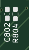
- If neither is possible, use best judgement, but remain consistent
- Headers
- All header pins must be labeled with the name of the signal that they are transmitting
- Top side must have:
- Board name and version
- Designer (or designers') name
- Release date (MMM/YYYY)
- Blank box for serial number
- ISC logo, should be full car silhouette unless absolutely impossible
- Sponsor Logos, until further notice, all boards should have the Bay Area Circuits Logo on the front
- If necessary, warnings and special precautions
- Bottom Side:
- (optional, for now) Something fun, like a quote, lyrics, or custom drawing. Something to give the board a unique touch.
- If you put something like “muck Fichigan”, make sure it’s on the side of the board that won’t be visible when mounted, or under a component. (I'll be hard for Bay Area Circuits to show off our new boards on their Twitter when it says "muck Fichigan" right next to the BAC logo.)
- (optional, for now) Something fun, like a quote, lyrics, or custom drawing. Something to give the board a unique touch.
- Dimension Labels
- Your board must include dimension labels indicating the PCB height, PCB width, and both vertical and horizontal distances between mounting holes
- example


Test Points
Test points make it easier to check signals and voltages on your board. They are a pad or hole in the board that is electrically connected to a signal and allows you to easily probe that signal and check it on a meter or oscilloscope.
Git Checks
All Git pull requests are automatically checked for correctness. Tnis ensures title blocks are correctly made, however these checks sometimes fail without apparent cause. If you cannot resolve the check, try this: Git Check Failure
Physical Board Dimensions and Shape
Using standardized dimensions makes it much easier for the Mechanical team to measure out and drill the mounting holes in the vehicle. Most times you will have some flexibility with hole spacing, other times it may be defined by a through-hole connector on the board. Verify your parts before you start.
- Mounting Holes
- Verify that the hole footprints from your schematic are "MountingHole_3.2mm_M3"
- Mounting holes must be horizontally and vertically separated from each other in increments of 1/16” (0.0625”), but 1/8” (0.125”) or whole numbers are preferred.
- E.g. 2 3/16” (2.1875”) is good, 2 1/8” (2.125”) is better, 2.000” is best.
- If you need holes that are not directly horizontal or vertical from another hole, space them apart by horizontal and vertical vectors that follow these same rules.
- No using arbitrary hole spacing (2.2723”), or non-standard multiples 2 31/40 (2.775”)
- PCB Dimensions
- This is a little more flexible than with mounting holes because most times your board just has to fit into a predetermined space.
- Board dimensions must end in either 5 or 0, and should be as close to multiples of 1/16" as possible.
- E.g. 2.775” x 2.000”, not 2.784” x 2.038”
- If it's close, consider rounding it up or down to a nicer number.
- E.g. Round 2.015" to 2.000" or 2.0625"
- Non-standard multiples are ok for board dimensions
- PCB Shape
- Try to stick to rectangular or square, but it's ok to use a different shape if your project needs it.
- Corners should be rounded off. Use the arc tool for this until they add rounded rectangles to KiCad.
Gerbers and DFM
When you are finished or nearly finished with your layout review, you will need to generate gerbers and run BAC's InstantDFM.
Further Reading
Adding_Symbols_&_Footprints_to_KiCad
Bay Area Circuits's standard capabilities.