| You are not Logged In! |
Difference between revisions of "Public:Schematic Conventions"
(Removed Notice about embedded images since images are now hosted on the wiki) |
|||
| (6 intermediate revisions by 4 users not shown) | |||
| Line 13: | Line 13: | ||
'''Be consistent with whatever conventions you choose, if we do not require a specific standard!''' | '''Be consistent with whatever conventions you choose, if we do not require a specific standard!''' | ||
| − | If you think something is hard to read or confusing, and you are following whatever conventions listed here, please post your dilemma in the | + | If you think something is hard to read or confusing, and you are following whatever conventions listed here, please post your dilemma in the {{SlackLink|elec-cad}} channel on [[Slack]]. |
| + | |||
| + | == Title Blocks / Page Information == | ||
| + | The Title Block on a Schematic (and PCB) is the information about the project shown in the bottom right corner of the page. The title block can be edited by clicking the "Edit Page Settings" in the top left on the tool bar. To keep information consistent and present between projects please follow these guidelines on the title block: | ||
| + | * '''Page Size:''' US Letter | ||
| + | * '''Title:''' The Name of the board, followed by hierarchical sheet name if applicable | ||
| + | * '''Comment 1: <code>Designed by: <your name(s)></code>''' | ||
| + | * '''Company:''' Illini Solar Car | ||
| + | * '''Date:''' Fill this in (MM/DD/YYYY) by clicking the <code><<<</code> button. Keep updated as you work on the board | ||
| + | |||
| + | * Comments 2+: Not required, can be used as needed to specify if you took the schematic from a different board or what not | ||
==Net Naming== | ==Net Naming== | ||
| − | All nets with more than two pins should be named with a descriptive name. | + | All nets with more than two pins should be named with a descriptive name. (feel free to name others as well when useful) |
Net names should only contain capital letters, numbers, and certain symbols including underscores and plus or minus. Net names should never contain spaces. | Net names should only contain capital letters, numbers, and certain symbols including underscores and plus or minus. Net names should never contain spaces. | ||
| Line 278: | Line 288: | ||
| PTC RESET FUSE 30V 200MA 1206 | | PTC RESET FUSE 30V 200MA 1206 | ||
| | | | ||
| + | |- | ||
| + | |Connector Through Hole | ||
| + | |CONN HEADER [orientation] [positions] [pitch] | ||
| + | |CONN HEADER R/A 4POS 2.54MM | ||
| + | |Use VERT for vertical, and R/A for horizontal. KK connectors have pitch 2.54mm, picoblade have 1.25mm | ||
| + | |- | ||
| + | |Connector SMD | ||
| + | |CONN HEADER SMD [orientation] [positions] [pitch] | ||
| + | |CONN HEADER SMD 2POS 1.25MM | ||
| + | |Leave blank for vertical orientation and use R/A for horizontal | ||
|} | |} | ||
| Line 309: | Line 329: | ||
[[File:Correct conn.png|frameless|200x200px]] | [[File:Correct conn.png|frameless|200x200px]] | ||
| − | ==Making Your Own== | + | ==Downloading or Making Your Own== |
| + | [[Adding_Symbols_%26_Footprints_to_KiCad]] | ||
| + | |||
| + | == Plotting Your Schematic == | ||
| + | To make viewing of schematics simple after your board has been manufactured please include a PDF of your schematic in your Pull Request after your design is complete. | ||
| + | |||
| + | To do so | ||
| − | + | # Open your KiCAD schematic | |
| + | # Press Plot [[File:Kicad Plot.png]] | ||
| + | # Use the following settings <br />[[File:KiCAD Plot Settings.png]] | ||
| + | # A PDF named <code>Project_Name.pdf</code> will be created in the project directory | ||
| + | # Commit and push the PDF | ||
=Recommended Reading= | =Recommended Reading= | ||
Latest revision as of 18:35, 20 March 2025
See Layout Standards for related information about developing your layout properly once the schematic is done.
See KiCad for information on setting up the latest supported version of the software before you get to work on these things.
Our team is in the process of creating and implementing standards for all of our electrical design and CAD. This is being done in an attempt to reduce errors in manufactured boards, make it easier for other members to edit boards that were already created, and make the finished CAD look presentable. Follow all conventions given here and be aware they may not cover all situations, as these standards are still a work in progress.
| Units | |
| Millimeters are fantastic and we encourage using metric dimensions whenever possible, however BAC's standards are written in mils (1/1000 inch) or inches so we present all minimum and recommended dimensions in both mm and mil. | |
General Advice for Clean Schematics
Be consistent with whatever conventions you choose, if we do not require a specific standard!
If you think something is hard to read or confusing, and you are following whatever conventions listed here, please post your dilemma in the ![]() elec-cad channel on Slack.
elec-cad channel on Slack.
Title Blocks / Page Information
The Title Block on a Schematic (and PCB) is the information about the project shown in the bottom right corner of the page. The title block can be edited by clicking the "Edit Page Settings" in the top left on the tool bar. To keep information consistent and present between projects please follow these guidelines on the title block:
- Page Size: US Letter
- Title: The Name of the board, followed by hierarchical sheet name if applicable
- Comment 1:
Designed by: <your name(s)> - Company: Illini Solar Car
- Date: Fill this in (MM/DD/YYYY) by clicking the
<<<button. Keep updated as you work on the board
- Comments 2+: Not required, can be used as needed to specify if you took the schematic from a different board or what not
Net Naming
All nets with more than two pins should be named with a descriptive name. (feel free to name others as well when useful)
Net names should only contain capital letters, numbers, and certain symbols including underscores and plus or minus. Net names should never contain spaces.
More guidance on net naming will be provided at a later time
Power Rails
No VCC/VDD. Net names should indicate the polarity and voltage of the rail. If the zero voltage reference of the rail is not the net named "GND", the net name of the power rail must reflect this.
- Voltage Rail should be near the top of the schematic
- *Voltage symbol usually points upwards
- *In the case of a voltage output, e.g. from a DC/DC converter, voltage symbol may point sideways
- GND Rail should be near/at bottom
- *GND symbol always points downwards
- If there is a decimal point in the voltage, use the convention of replacing the decimal with V for voltage, e.g. +3V3 describes +3.3V
I2C/SPI
Will expand on this later
UART
It is very easy to get mixed up with UART nets, be thorough and double check your work!
UARTx_Source_to_Destination
Examples
Put some examples here
Graphical Considerations
Schematics are the most critical piece of documentation for a PCB. They are read by both ECAD software and fellow engineers. The schematic should clearly illustrate its functionality, be easy to read, and contain enough information so that it is easy to order parts and assemble the finished PCB.
More information will be provided at a later time
Sheets
Paper size
ANSI A (8.5" x 11")
We need to be able to print out all of our current schematics at any time as a backup.
Diptrace archives may not use any standard paper size, as we did not enforce the standard on our boards when we used it.
How to set the correct size:
- Click the "Edit Page settings" icon:

- Make sure "A 8.5x11in" and "Landscape" are selected
- All of the other options should be changed per page, more on those in Title Block
How to export the pages to PDF for printing:
- Click the Plot Schematic icon:

- Make sure the output setting is PDF
- Click "Plot All Pages"
Title Block
Kicad Default, Diptrace --TBD-- now defunct, do not use
Include information in these fields:
Coming soon...
Wire Crossings
Long answer short, dots on all 3-way intersections, no dots on 4-way intersections. A dot means that the wires connect, no dot means that there's no connection. Keep reading to find out why those statements should not contradict each other in your design. If you encounter a 4-way connection, in which both wires crossing at the perpendicular angle are connected to each other, separate it into two 3-way connections instead.
Take a look at these pictures for some examples:

- Left vertical wire connects to 3 but not 1.
- Right vertical wire connects to 1 only
- 2 connected to GND and not 3

- Left vertical wire connects to 3 but not 1
- Right vertical wire connects to 1 only
- 2 needed to connect to both 3 and GND, so that's separated into 2 different connections: 3 to GND and 2 to 3
- Do not simply put a dot on the 4-way intersection to show the connection between 3, GND, and 2
Direct Wire Connections
Wires should be as straight as possible to make it easier for the eye to follow.
Routing from Components
Route lines should come straight out of components, as opposed to immediately making an angle. This makes it easier to move components later on.

Prevent Overlapping
Components, reference designators, and part values must never overlap anything. The only thing that wires can cross is other wires. Text comments should not overlap anything.
Net Coloring
While net coloring can be useful to easily identity and follow nets around a schematic, the schematic should be completely intelligible without net coloring. This is because the schematic will most likely be printed in black and white if it is printed.
We chose the fields to add the least amount of work possible to making schematics, while still including all the necessary information for sourcing and placing components and working with BOM mangement software. Please give feedback on anything you want clarified or changed, on the #elec-cad channel on Slack.
Part Information
The schematic needs to include all of information needed to specify the characteristics of every part used on the board. To do so, the schematic fields should be filled in completely for each part as applicable. There are seven fields we use. KiCad will not default to these seven so you must add them so that you have the defaults plus: MPN, DNP, Note . To do so:
Windows: Do this by opening Eeschema and going to Preferences -> General Options and the Field Name Templates tab.
Mac: Do this by opening Eeschema and going to KiCad -> Preferences -> General Options and the Field Name Templates tab.
You can also choose whether or not it is visible on the schematic by default, and you can change any field's visibility as you edit each part. Pro tip! Go to Tools --> Edit Symbol Fields... to see all the fields for all the parts and edit them in what's basically a spreadsheet but slightly more annoying. (It's still easier than trying to remember which parts you edited individually.)
Following are the standards to be followed for the information required to be in each field
The standards are intended to ensure that every part on the board is clearly specified, standardize the information across projects, and ensure compatibility with other tools and ordering.
| Name | Default? | Required on every part? | Include in Field | Not Allowed in Field | Additional Notes / Motivation |
|---|---|---|---|---|---|
| Reference | Y | Y | Automatically generated | You can change the refdes numbers yourself too. This may be useful if, for example, there are a series of outputs and you want the refdes numbering to correlated to the output number. Set those first and them have KiCad assign the rest. This is how specific parts are identified on the board | |
| Value | Y | N | This will be included on most parts. Cap: Farads |
Anything else | This is the inherent value of the part you need. The most important or descriptive value for the type of part it is. This should, at a glance, give someone the info they need to parse the schematic function. Specifics for implementation will be elsewhere. |
| Footprint | Y | Y | Assigned when a footprint is selected in the browser or preassigned for parts with only one footprint | Anything that's not a footprint in our libraries | Everything needs a footprint (even if it won't be populated) so that it can be put on the layout. |
| MPN | N | Y | This is the part number for the part. For ICs or other specific components (such as connectors, specialty parts) this will be the manufacturers part number. For discrete components with many equivalents see the below table for the part number details | This is the part number used for BOM and inventory purposes especially with PartsBox. This should be the same as what the Part Name would be in PartsBox (i.e. copy it from there if you aren't sure what to do). For the discrete parts it is the name of the meta part that includes all the appropriate equivalents. If this is not a part with a meta part naming format listed below you should use the manufacturers part number! | |
| DNP | N | N | DNP or Blank | Anything else | If a part should not, for whatever reason, be populated put that in the field. Anything other than blank is interpreted as DNP |
| Note | N | N | Any implementation details, other notes on part selection, function notes (e.g. CAN LED, 12V Input, Etc) | Info that is included above | Any labels that you would put to clarify the function of the part in the schematic should go here and then you can show the field to make it visible on the schematic |
MPN for non-specific parts
This is motivated by the need to have the specific identifier for all parts in a field for simpler PartsBox integration and compatibility. Additionally, it will ensure that the specifics of these parts is considered and determined - there will be enough info to get the correct part without assumptions. The following table lists the discrete parts that we have generic parts (Meta Parts) for since there are lots of drop in replacements. Other parts should all have the MPN listed for MPN.
| Part type | Format | Example | Notes |
|---|---|---|---|
| Resistor (surface mount) | RES SMD [ohm rating] OHM [tolerance] [power rating] [size] | RES SMD 10K OHM 1% 1/4W 0603 | |
| Resistor (through hole) | RES [ohm rating] OHM [tolerance] [power rating] AXIAL | RES 10K OHM 1/4W 5% AXIAL | |
| Capacitors (ceramic) | CAP CER [farad rating]F [voltage rating] [temp. response code] [size] | CAP CER 0.047UF 50V X7R 0603 | The temp response codes C0G and NPO are used interchangeably or in tandem (i.e. C0G/NP0). Please use C0G for these parts regardless of the Digikey listing |
| Capacitors (electrolytic) | CAP ALUM [farad rating]F [tolerance] [voltage rating] RADIAL | CAP ALUM 33UF 20% 35V RADIAL | DigiKeys descriptions seems to be less consistent for these than other parts |
| LEDs (generic SMD) | LED [led color] [lens color] [size] SMD | LED BLUE CLEAR 0603 SMD | This is for, typically, on-board LED indicators. Other LEDs (such as car lights) need specific part numbers |
| LEDs (generic THT) | LED [LED color] [lens color] [radius] ROUND T/H | LED GREEN CLEAR 5MM ROUND T/H | |
| Diode Schottky | DIODE SCHOTTKY [voltage rating] [current rating] [package] | DIODE SCHOTTKY 30V 200MA SOD523 | Note that there may be different names for the same package. Please check! |
| TVS Diode | TVS DIODE [reverse standoff voltage rating] [clamping voltage] [package] | TVS DIODE 24V 50V SOT323 | Note that there may be different names for the same package. Please check! |
| Diode Zener | DIODE ZENER [voltage rating] [power rating] [package] | DIODE ZENER 10V 500MW SOD123F | Note that there may be different names for the same package. Please check! |
| Diode (general) | DIODE GEN PURP [voltage rating] [current rating] [package] | DIODE GEN PURP 200V 2A SMA | Note that there may be different names for the same package. Please check! |
| Fuse (glass) | FUSE GLASS [current rating] [voltage rating] [size] | FUSE GLASS 1A 250VAC 5X20MM | |
| Fuse board mount no holder | FUSE BOARD MNT [current rating] [voltage rating ac] [voltage rating dc] | FUSE BOARD MNT 2A 350VAC 72VDC | Note that if the AC/DC rating are the same you should combine them as in the example for the fuse with holder |
| Fuse board mount with holder | FUSE BOARD MNT [current rating] [voltage rating ac] [voltage rating dc] SMD | FUSE BOARD MNT 2A 125VAC/VDC SMD | Your board always needs a holder so use this, the previous is for replacement fuses! |
| Fuse SMD (generic) | FUSE BOARD MNT [current rating] [voltage rating] [size] | FUSE BOARD MNT 1A 32VDC 0603 | The abbreviation of Mount is inconsistent on digikey. Use MNT |
| Fuse SMD PTC | PTC RESET FUSE [voltage rating] [current rating] [size] | PTC RESET FUSE 30V 200MA 1206 | |
| Connector Through Hole | CONN HEADER [orientation] [positions] [pitch] | CONN HEADER R/A 4POS 2.54MM | Use VERT for vertical, and R/A for horizontal. KK connectors have pitch 2.54mm, picoblade have 1.25mm |
| Connector SMD | CONN HEADER SMD [orientation] [positions] [pitch] | CONN HEADER SMD 2POS 1.25MM | Leave blank for vertical orientation and use R/A for horizontal |
Note: these formats were taken from Digikeys standard part descriptions. Therefore, if a part doesn't exist in partsbox and you aren't sure what the MPN should be exactly you can look there for reference (although beware that if you spend enough time on digikey you will run into errors - they appreciate it when you report these errors (:smile:))
Note 2: For those that use package names, the names are stylized without the dash between letters and numbers but with any dashes between numbers. i.e. SOT-323 becomes SOT323 and SOT-23-3 becomes SOT23-3. You will see both conventions used in various places
We chose the fields to add the least amount of work possible to making schematics, while still including all the necessary information for sourcing and placing components and working with BOM mangement software. Please give feedback on anything you want clarified or changed, on the #elec-cad channel on Slack.
Symbols
Using Them
Capacitors
Below is a diagram of the correct and incorrect capacitor symbols. Never use the small capacitor symbols. You do not need to. Only use the polarized symbol if you have a capacitor which is polarized, such as an electrolytic cap. Ceramic capacitors are the ones used most often on our PCBs, and they are not polarized.

Resistors
Like the picture of the capacitors above, never use the small resistors symbols. This is to keep the resistor size the same across all our boards. Also, make sure to keep the style of your resistors the same throughout your schematic whether that is the US or the European style.
Connectors
Please do not use these connector symbols:

Instead, use these connector symbols:

Downloading or Making Your Own
Adding_Symbols_&_Footprints_to_KiCad
Plotting Your Schematic
To make viewing of schematics simple after your board has been manufactured please include a PDF of your schematic in your Pull Request after your design is complete.
To do so
- Open your KiCAD schematic
- Press Plot

- Use the following settings
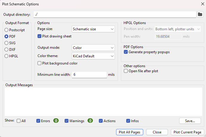
- A PDF named
Project_Name.pdfwill be created in the project directory - Commit and push the PDF
